

By
45 min ago 2 min read
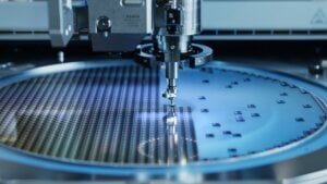
Tessalia Technology (Tessalia), a semiconductor packaging joint venture between Foxconn, Radiall, and Thales, has outlined plans for an advanced semiconductor packaging facility in Le Barp, Nouvelle-Aquitaine, to strengthen French and European competitiveness in the global semiconductor market.
The Le Barp site could attract more than €250m ($291m) in investment by 2033, with system-in-package (SiP) component production expected to begin at the end of 2029.
Tessalia aims to produce more than 50 million SiP components annually by 2033.
The target is, however, lower than that outlined during preliminary discussions held in May 2025, when the partners said the facility could produce more than 100 million SiP components annually by 2031.
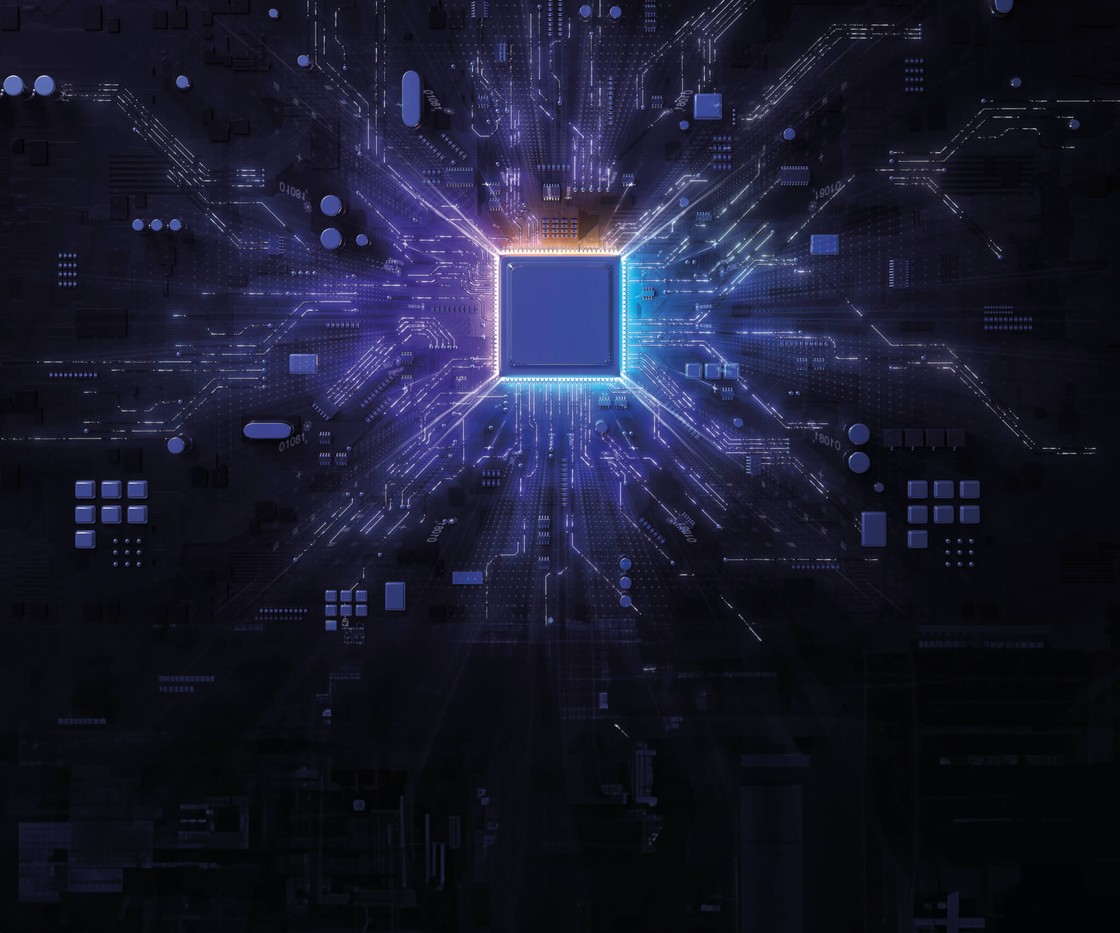
SiP technology integrates multiple semiconductor components into a single package and is used across aerospace, telecommunications, medical and automotive applications.
At the site, Tessalia plans to deploy encapsulation technology designed to produce ultra-high-density SiP components, enabling smaller and lighter electronic assemblies with improved integration capabilities.
The company will operate as an outsourced semiconductor assembly and testing (OSAT) provider.
Young Liu, Chairman of Foxconn, said, “This [joint venture] is not just a factory…It is a strategic platform for advanced manufacturing, semiconductor resilience, and future technologies in Europe.”
The joint venture will have access to Foxconn’s semiconductor technology through licensing arrangements.
Patrice Caine, Chairman and CEO of Thales, said Tessalia represents a push for control over the company’s electronics value chain amid a competitive global semiconductor market.
The announcement follows French President Emmanuel Macron’s at the French Alternative Energies and Atomic Energy Commission (CEA), where he stated the next two years are critical for strengthening the European semiconductor value chain to remain competitive in the global market.


