

By
49 min ago 2 min read
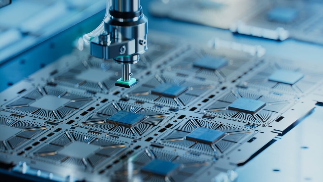
Japanese semiconductor manufacturer Resonac has launched a semiconductor packaging research and development (R&D) centre in Silicon Valley, California.
The opening marks the full-scale launch of the US-JOINT consortium – formed of 12 Japanese and US materials and equipment manufacturers – aimed at accelerating next-generation chip packaging development.
US-JOINT says the site is the first of its kind in the US.
Hidehito Takahashi, President and CEO of Resonac, said the US-JOINT group wants to shorten the proof-of-concept period from around six months to as little as one month.
To do this, the consortium will collaborate with major users of advanced semiconductors.
US-JOINT was first . It will utilise each company’s technology, materials and equipment to advance semiconductor development and support rapid testing, commercial scaling, and distribution of its packaging technologies.
Kazumi Nishikawa, Director-General for Economic Security Policy, Trade and Economic Security Bureau, Ministry of Economy, Trade and Industry, said the growth of AI has for advanced packaging technologies.
“I am very confident that US-JOINT is just the start of innovation for advanced packaging and chiplets in generative AI computing,” he adds.
Advanced semiconductor packaging is central to generative AI, autonomous driving, and increasingly, it is being used by IT companies to customise their own AI technology.
US-JOINT is formed of Resonac Corporation, Azimuth Industrial, KLA Corporation, Kulicke and Soffa Industries, MEC, Moses Lake Industries, Namics Corporation, Tokyo Ohka Kogyo, Toppan, TOWA Corporation, ULVAC, and 3M.


